[ad_1]
This is the continuation of a series of posts where I create a schematic and PCB in various EDA tools. Already, we’ve looked at Eagle CAD, KiCad, and took a walk down memory lane with one of the first PCB design tools for the IBM PC with Protel Autotrax. One of the more controversial of these tutorials was my post on Fritzing. Fritzing is a terrible tool that you should not use, but before I get to that, I need to back up and explain what this series of posts is all about.
The introduction to this series of posts laid it out pretty bare. For each post in this series, I will take a reference schematic for a small, USB-enabled ATtiny85 development board. I recreate the schematic, recreate the board, and build a new symbol and footprint in each piece of software. That last part — making a new symbol and footprint — is a point of contention for Fritzing users. You cannot create a completely new part in Fritzing. That’s a quote straight from the devs. For a PCB design tool, it’s a baffling decision, and I don’t know if I can call Fritzing a PCB design tool now.
Contextualizing this Whole Mess
If you’re like the majority of desktop or laptop users, the easiest tool to make pixel art is Microsoft Paint. With MS Paint, you can edit individual pixels, select colors, and even do flood fills. It’s exactly what you need if you want to create pixel art quickly with a tool that’s easy to use. There are better tools to create pixel art, though. Photoshop lets you zoom in to see individual pixels and has transparency and layers, and Aseprite is a professional tool specifically designed for the creation and animation of pixel art.
It’s easy to draw parallels between KiCad, Fritzing, MS Paint, Photoshop, and Aseprite. Fritzing and MS Paint are easy-to-learn tools where you can produce acceptable results quickly. This is a false equivalency, though; you can do anything you want in MS Paint, but you can’t do anything you want in Fritzing because you can’t add custom parts. Fritzing is a tool just like MS Paint if MS Paint didn’t have the color blue.
Creating a custom part is necessary functionality of a PCB design tool. The first PCB design tool released for the PC had this functionality. Without the ability to create custom parts, Fritzing cannot legitimately call itself a PCB design tool and should not be used as such.
Of Course You Can Make Custom Parts (It’s Just Tedious)
The Fritzing FAQ is wrong. Of course you can make custom parts in Fritzing. This summer, Adafruit created a whole bunch of Fritzing parts that still haven’t been added to the core libraries. Instead of complaining about the relatively small core library, or the difficulty in adding custom parts, I’m going to do something better: for the next two thousand words, I’m going to demonstrate how to create a custom part in Fritzing.
It should be noted that since the introduction of the new Fritzing Parts Editor introduced in version 0.7.9 (the version that took away the ability to create custom parts), there have been no tutorials on how to create a custom part in Fritzing. This is the first such tutorial and by definition the best tutorial on creating custom parts in Fritzing. I encourage the Fritzing team to post a link to this tutorial on their blog and FAQ.
With the justification of why you should never use Fritzing and why this tutorial is necessary, let’s begin. This is how you create a custom part in Fritzing.
The Easy, Dumb Way
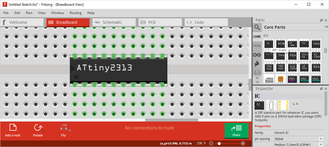
The picture above is of an ATtiny2313, a part not in the Fritzing core library. I created this part in just a few minutes using tools built right into Fritzing. Yes, you can make your own parts in Fritzing. Here’s how I did it.
 From Fritzing’s ‘Core Parts’ selector, take the generic IC part and drop it onto the breadboard view. In the Inspector window, you will find options for what type of package this part is, how many pins, it’s label, and even the pin spacing. If you want to drop a 40-pin CERDIP 6502 into your Fritzing project, you can do that. If you want to drop a 64-pin Motorola 68000 into your Fritzing project you can do that. If, for some reason, you want to add an IC that isn’t in the core Fritzing library, you can do that too. All of this is done semi-automagically by Fritzing. All you need to do is tell Fritzing the number of pins, and what package it comes in.

What’s the bottom line? If you’re dealing with a DIP chip, a QFN, SOIC, or some other standard package, you can probably make a Fritzing part in about three minutes. Is this making a part from scratch? No, but for most use cases, this is all you need.
Actually Creating A Part From Scratch
The challenge for this tutorial was to create a part from scratch. To that end, I’m going to build a purple and gold 64-pin DIP Motorola 68000. Why not, right?

Step 1: Creating A Breadboard Footprint
Download Inkscape. It’s like Illustrator, only it doesn’t send your soul back to the Adobe mothership. Select File -> Document Properties, and set the size of the canvas to 3.2 x .98 inches. While you’re in that window, set the default measurement unit to ‘inches’.
The width of the canvas is the nominal width of the package, and the height will be the nominal height of the package plus space for the pins. The pins will be squares with a dimension of 0.04 x 0.04 inches, so add 0.08 inches to the top and bottom of the canvas.
With the dimensions of the canvas set, draw a rectangle. If you’re feeling exceptionally artistic, make the rectangle purple and add some gold accents. Now it’s time to add pins. This is a 64-pin device, so add sixty-four rectangles. Use Inkscape to arrange and distribute them logically. In Inkscape’s ‘Object Properties’ window (Shift+Ctrl+O), set the ID of each rectangle to ‘connector0pin’ to ‘connector63pin’. Yes, Fritzing uses zero-indexed numbers to label all the pins on the breadboard view.

Once all the pins are labeled, select all, group everything and name this group ‘breadboard’ in the Object Properties window. Save this file to your desktop as a plain SVG (not an Inkscape SVG). That’s it for the Inkscape portion of building the breadboard part. Now we take it over to Fritzing.
In Fritzing, create a new part just like you did in the ‘Easy, Dumb Way’ above. In the Parts Editor, select File -> Load Image For View, and select the SVG you just saved from Inkscape. You’ll get something that looks like this:

Yes, the font changed, but whatever. This is the closest anyone has ever gotten to building a custom part in Fritzing. On the right side of the screen, there’s a list of connectors, with a button labeled ‘select graphic’ next to each pin. For each pin on our 64-pin monster, click the ‘select graphic’ button, and then click the gray rectangle of the corresponding pin. This shouldn’t be necessary if you labeled your parts correctly in Fritzing, but it’s another option for you.
Save the part, open up a new Fritzing window, and here’s what you get:

To reiterate, this is a custom part, with a custom breadboard view. There are no other tutorials that tell you how to do this. You’re welcome.
Step 2: Creating The Schematic Footprint
The breadboard view is only one-third of what’s required to make a part in Fritzing. Now we’re going to move on to the schematic view. This is a simplified view of the part that shows the functions of all the pins.
 First, create a new Inkscape document with a width of 1.5 inches and a height of 3.3 inches. If you’re making a DIP schematic, the formula to calculate the height of a part is ([number of pins on one side] + 1) * 0.1. For a 64-pin chip with 32 pins on a side, it’s 33*0.1 = 3.3.
The body of the schematic footprint is a rectangle, no fill, black outline, with a 1px stroke width. The pins are a straight line, 0.25 inches long, arranged along the side of the black rectangle on 0.1″ centers.
Right now we have a simplified version of what the schematic footprint should look like. Yes, we’re missing labels for all the pins, but something even more important is missing: the IC terminals, or where the lines on the schematic connect to. Fritzing thinks these should be rectangles 0.2 pixels square (yes, point two pixels), so we need to add these to the end of every pin on this footprint.
Create a 0.2 by 0.2 pixel rectangle on the tip of every leg of the schematic, and label them in the Object Properties dialog as ‘connector0terminal’ through ‘connector63terminal’. Once that’s done, label the pins in the Object Properties dialog as ‘connector0pin’ through ‘connector63pin’. Yes, that’s one hundred and twenty-eight things you need to rename. It’ll take a while. When that’s done, save it as an SVG, go to the parts editor in fritzing, and select File -> Load Image For View and choose the file you just created in Inkscape. Here’s what you’ll get:
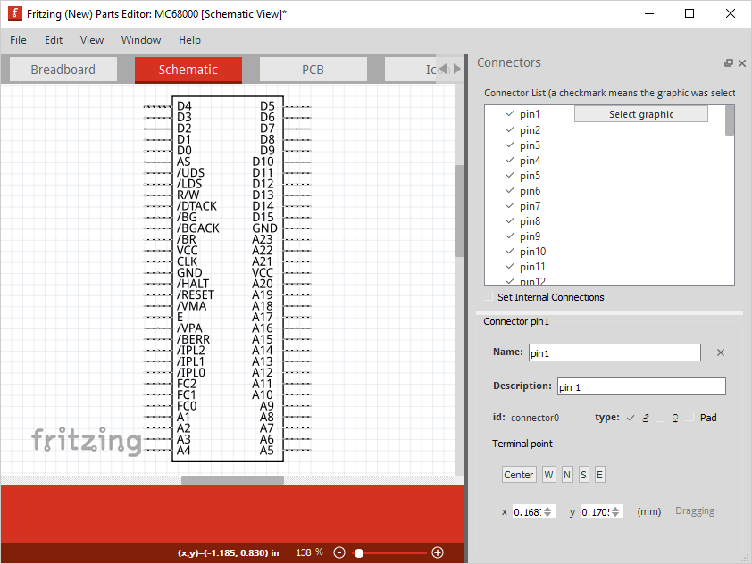
I’ve added a few things to this schematic view, most obvious is the pin labels. Other than that, it’s pretty standard, and now we’re almost done creating a part from scratch in Fritzing.
Step 3: Creating The PCB Footprint
You know the drill by now. Create a new Inkscape document. The dimensions of the canvas are (width of the package + 0.02 inches) by (height of the package + 0.02 inches). For the 68000, that’s 3.22 inches by 0.92 inches. Your pads are just circles, with no fill, and some sort of yellow stroke. Arranging these pads is left as an exercise to the reader.
Fritzing requires you to name these pads, so name them ‘connector0pin’ through ‘connector63pin’. Group all of these pads and call that group ‘copper0’, then group them again and call that group ‘copper1’. This is, ostensibly, for the top and bottom copper layers.

Save this as a regular SVG, open up Fritzing, go to the Part Editor, and replace the PCB footprint with the SVG you just saved.

With that, we’re done. That’s how you create a part mostly from scratch in Fritzing. Hit save, close Fritzing, and throw your computer in the garbage. It’s tainted now.
What this all means

Admittedly, I didn’t make this easy on myself by creating a 64-pin DIP from scratch in Fritzing. Making a part in Fritzing is a tedious process and should not be done by anyone. It’s possible, though, and if you have enough time on your hands, you can create beautiful vector graphics that are also real, working parts in Fritzing.
Supporters of Fritzing say its greatest strength is that it’s an easy tool to use, and useful if you want to whip up a quick PCB for prototyping. They are correct, so long as all the parts you want to use are already in Fritzing’s core libraries. It is possible to create parts from scratch, but this is a task that could be done faster in literally any other PCB design program. What we’re looking at here is a walled garden problem, and for the second most popular Open Source PCB design software, this isn’t doing Fritzing any favors.
It should be noted, however, that many of the tasks required to make a Fritzing part can be automated. PCB and schematic footprints can be auto-generated. In theory, a simple command line tool could tie these parts directly to breadboard footprints. If anyone wants to contribute to Open Source in a meaningful way, there’s a project for you: make a tool that takes an SVG of a chip or component and turns it into a Fritzing part.
Closing out this tutorial, I’d like to thank [Arsenijs] who created the first tutorial on making a Fritzing part over on Hackaday.io. [Arsenijs] did this because I put up a bounty for the first guide to making a part in Fritzing from scratch. Not only do I contribute to Open Source (which means I’m better than you), I contribute to Open Source documentation. I am a unicorn that lays golden eggs.
That’s it for Fritzing. I’m not touching it again. For the next post in this Creating a PCB in Everything series, I’m going to take a look at the cloud-based PCB design tool, Upverter. Will it be better than Fritzing? Who knows. Maybe. Probably.
[ad_2]
Source link


